UV and LED Technology for Printed Electronics
Press release from the issuing company
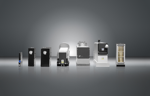
At the LOPEC IST Metz presents its wide product portfolio of highperformance UV and LED curing units.
LOPEC 2022: IST METZ presents water and air-cooled UV technology in different performance classes
Nürtingen: At the LOPEC, which takes place from 23. to 24. March in Munich, UV equipment manufacturer IST METZ will present the latest UV and LED units for fast and reliable curing of printed circuits.
MBS-LI for thermally sensitive materials With a maximum lamp length of 550 mm, the high-performance MBS LI unit achieves a maximum output of 270 W/cm. An optimized air flow and the use of a quartz glass pane between the lamp chamber and the substrate guarantee effective heat management in the UV system and enable the MBS LI to be used even with temperature-sensitive materials.
LED technology in printed electronics In addition to its portfolio of classic medium pressure steam lamps, IST Metz, together with its subsidiary Integration Technology, will also be presenting the latest LED technology. The systems consist of freely configurable and addressable modular units which can be adapted to the specific requirements of the respective application. This ensures optimum curing without affecting the substrate. The SPOTcure series for precise curing is also part of the LED product portfolio. The high-power, multispectral systems combine the radiant power and spectral characteristics of a mercury arc lamp with the TCO and process advantages of LED technology. The handheld HANDcure also enables the user to work mobile and fatigue-free wherever controlled curing and immediate handling stability are required.
Cleaning and modification through Excimer technology
UV cleaning methods play a key role in the display and semiconductor sector. Very short wavelength UV light (peak value 172 nm) is used to break up the bonds in organic substances. Additional generation of ozone oxidizes these contaminants into carbon dioxide and water. The result is a clean surface. The modification of surfaces improves surface tension, which in turn improves wettability. Wettability is measured via contact angle. A significant effect is achieved at wavelengths of below 200 nm. Spheres of application: display panel production, touch panel production, wafer production.
- Questions to ask about inkjet for corrugated packaging
- Can Chinese OEMs challenge Western manufacturers?
- The #1 Question When Selling Inkjet
- Integrator perspective on Konica Minolta printheads
- Surfing the Waves of Inkjet
- Kyocera Nixka talks inkjet integration trends
- B2B Customer Tours
- Keeping Inkjet Tickled Pink
© 2024 WhatTheyThink. All Rights Reserved.


