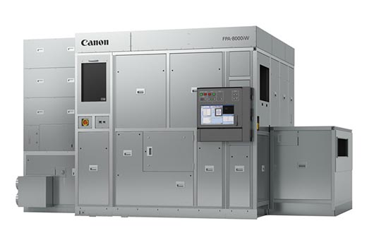
Canon to Commence Sales of the FPA-8000iW Semiconductor Lithography System Which is Capable of 1 micron Resolution with Support for Large Panels
Press release from the issuing company
Melville, N.Y. – Canon U.S.A., Inc. today announced that its parent company, Canon Inc., expects to commence sales in early July 2020 of the FPA-8000iW i-line stepper1, a new Semiconductor Lithography System for advanced chip packaging. This system combines fine 1 μm2 resolution with support for customer’s large panel substrates with sizes up to 515 x 510 mm.
This new product marks the first Canon Semiconductor Lithography system to support manufacturing using large panels that are common in back-end processing. Integrating a Canon proprietary projection optical system, the FPA-8000iW offers a wide exposure field and fine 1 μm pattern resolution. The FPA-8000iW was designed to meet the needs of manufacturers who are aiming for high-production efficiency by using 515 x 510 mm organic (e.g., carbon based) panel substrates for Panel Level Packaging (PLP) applications. PLP processes typically involve mounting and processing a large number of semiconductor chips on large, thin panels to produce packages that can help increase communication bandwidth and reduce power consumption of high performance computing systems.
Future customer requirements for PLP processes include cost reduction and further shrinking of semiconductor packaging that can help protect delicate internal semiconductor circuity from outside environments and electrically connects to external components. The FPA-8000iW supports PLP cost reduction and package scaling by providing high-productivity panel processing with a large exposure field and high resolution.
In response to packaging processes that use panel substrates, Canon developed this new FPA-8000 Body platform capable of handling large 515 x 510 mm panel substrates. Severe warpage is also common in large-panel substrates and the new platform and panel-feeding system can overcome up to 10 mm of panel warpage. As a result, the FPA-8000iW can help customers realize high-productivity and efficiency for PLP production of large packages.
The FPA-8000iW stepper employs Canon’s proprietary projection optical system that supports a wide 52 x 68 mm exposure field while achieving 1.0 μm resolution, which is the finest resolution among lithography systems that support large panel substrate processes3. As a result, advanced packaging technology such as PLP can help customers innovate to provide high integration and flexibility in electronic system design.
To keep apprised of the latest news from Canon U.S.A., sign up for the Company's RSS news feed by visiting www.usa.canon.com/rss and follow us on Twitter @CanonUSA.

- Questions to ask about inkjet for corrugated packaging
- Can Chinese OEMs challenge Western manufacturers?
- The #1 Question When Selling Inkjet
- Integrator perspective on Konica Minolta printheads
- Surfing the Waves of Inkjet
- Kyocera Nixka talks inkjet integration trends
- B2B Customer Tours
- Keeping Inkjet Tickled Pink
© 2024 WhatTheyThink. All Rights Reserved.


